
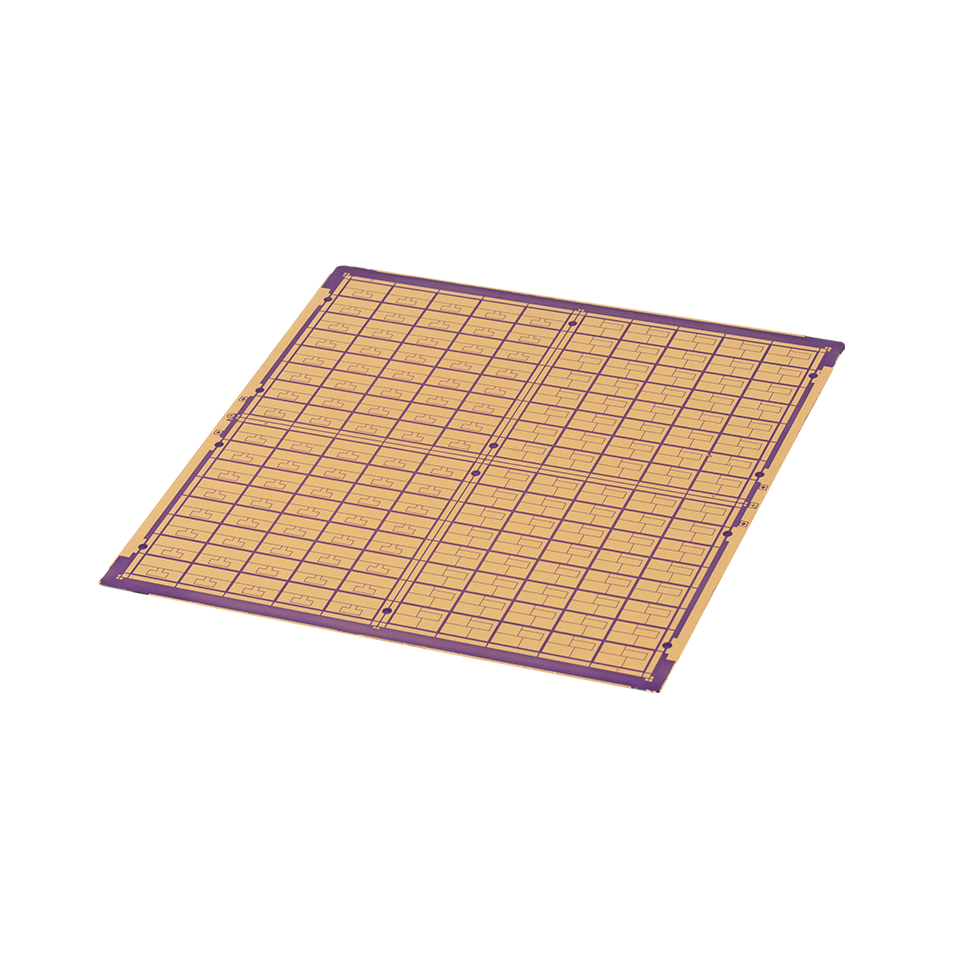
 Thin film ceramic heat dissipating substrate
-
Buy substrate material
Size: 5〜5.0"
Thickness: 0.38/0.5 mm
-
Laser via/precut
Dia.: 50~150um
-
Sputter Titanium Copper
Ti:0.1um
Cu:0.3~0.5um
-
Laminate
-
Photolithography & 3D dam
-
Plate copper
Copper thickness: 35~300um
Hole plating: 50~100um
-
Grind
Ra<0.5um
-
Plate Ni, Silver, Au
Ni: 3~7um
Au >0.1um
-
Defilm
-
Etch
-
Fit (Photolithography)
-
Clean
-
Inspect
-
Pack
Thin film substrate
JST has complete equipment and technology of thin-film process. Starting from the original substrate material, JST can work with customers to cope with the ever-changing technological trend of electronic heat-dissipating substrates through various processes of laser, grinding, etching, etc., and towards the diverse development of in-vehicle automation and the original universe.
The available production specifications are as follows:
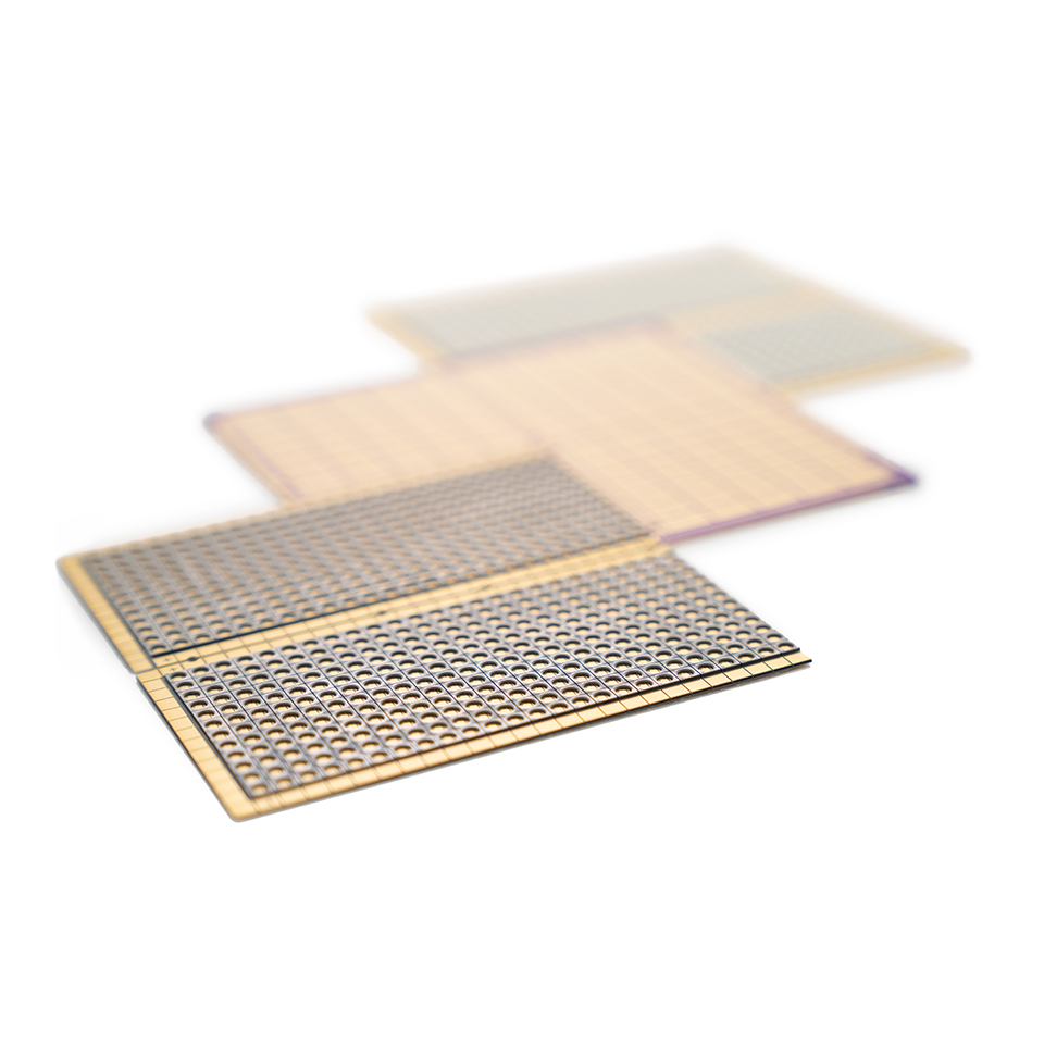 3D thin film substrate